Semiconductor Post Silicon Validation has always suffered from a lack of standardization. While the semiconductor design process has standardized tools and technologies, most organizations still depend on manual efforts and homegrown automation frameworks for validation and data collection. Data management is also often done with either Excel or other suboptimal database solutions. Over time, however, we observe that these home-grown solutions lose traction – either the original developers have moved on, or the frameworks become difficult to maintain due to all the features added over time.
We at Soliton have vast experience addressing these very issues. We have built standardized software frameworks and database infrastructure for numerous clients, including 5 of the top 10 mixed signal/analog semiconductor companies in the world, and over the years, our understanding has deepened. We have moved from simply building technology solutions to being consultants in this space. Using the Design Thinking Methodology, we have been able to engage in systematic studies with customers in recent months to identify problem areas – previously dismissed as non-existent or too minor to address, we have addressed them to make a large impact. This is the process we are sharing with you.
Our Design Thinking Engagement Model
Here are the high-level steps we use to help our Global Major customers around the world. Though the details might change case-by-case, we believe this post should provide an understanding of the process and merits of using the Design Thinking approach.
Step 1: An introduction to Design Thinking
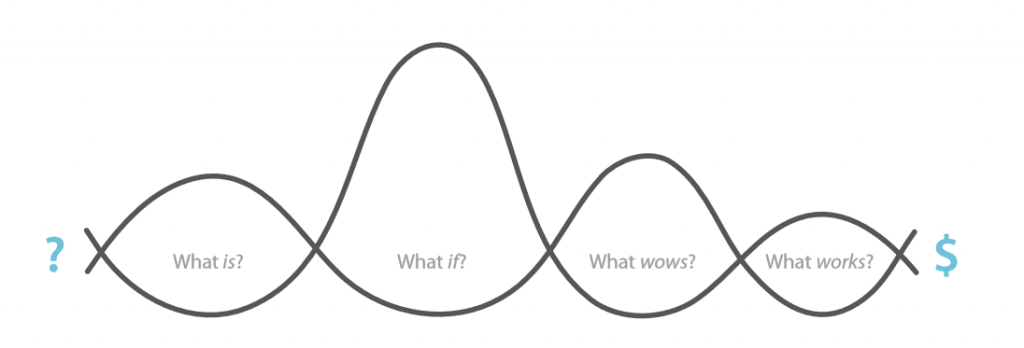
Figure 1: From the book “Designing for Growth: A Design Thinking Tool Kit for Managers” by Jeanne Liedtka and Tim Ogilvie
Design Thinking is relatively new to the Semiconductor Engineering community from what we have seen, and so a presentation introducing the topic could be helpful. We have found Figure 1 to be a very effective illustration for this purpose. As we walk through our process and show sample reports – many customers find that we are bringing a systematic approach to processes they might have pursued in a more ad-hoc or unstructured way in the past. However, some customers are turned off because the step-by-step nature of the Design Thinking methodology does not commit to specific results at this early stage.
Step 2: What is?
Once the basics of Design Thinking are covered, we do a deep-dive into the client’s organization through either shadowing employees or conducting interviews. By engaging with their employees at all levels and gaining insight into their work, we develop empathy and understanding of their needs. We have found that an appreciation of various aspects of their job – from their likes and dislikes to day-to-day moments of excitement and boredom – this is all essential information for creating a comprehensive solution for the client.
Mind Map
We then document and present our finding through a mind mapping exercise. Unlike a tradition mind map, we think of this exercise more as an ‘information yard sale’ which helps us to better frame the key problems that our solution needs to address.
User Journey Map
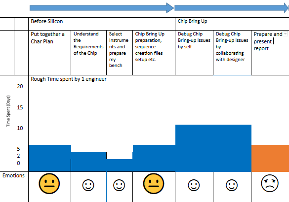
These findings are further developed into an attention-grabbing visual document that represents the amount of time that engineers spend on engaging and monotonous tasks respectively. Our experience has shown that Validation Engineers want to spend more time on core engineering activities. Through this User Journey Map, the client comes to see all the non-core activities that are taking away valuable time and resources, and we can focus on developing our tool to either eliminate or streamline these areas.
Design Criteria
This extensive ‘What Is’ phase produces a comprehensive Design Criteria document. Here are examples of findings from previous such documents:
- The System needs to help organize measurement data and enable instant access to historical data as and when needed.
- The System needs to organize validation assets such as sequences, instruments etc and allow me to reuse validation assets with the same ease as to how designers reuse IP block in design.
- The System needs to be intuitive and fast such that we get good adoption within the validation community.
- The Design Criteria Document serves as a game plan for the upcoming solution-building phase.
Step 3 and beyond
Subsequent stages of engagement with the client involve a Napkin Pitch, which is a more refined version of the Design Criteria Document that lays out our priorities for solution-building. Further brainstorming is involved in this stage.
At this point, we bring in a couple of new concepts: Lean Principles and Agile Methodology. These are outside the scope of this blog post, but the following article should outline the benefits of Lean Principles and Agile Methodology, and how they work with Design Thinking to achieve the goals we have set out thus far.
Conclusion
Design thinking provides a framework that lets us approach post-silicon validation problems in new and empathetic ways. Understanding the client’s struggles and emotions give us the perspective necessary to build the ideal solution for them.
This approach, however, is not without its challenges. It can be difficult to find engineers who are comfortable with being shadowed, and the alternative – conducting interviews – can prove to be less illuminating. In a large organization, validation engineers are globally distributed, which makes it difficult to cover the issues that arise in different geographic location. Again, we try to mitigate this by releasing an international survey to collect at least some information from these locations. Shadowing engineers, however, is the ideal process since it is also extremely time-efficient and helps us wrap up the ‘What Is’ stage very quickly.
We hope this blog post gave you an understanding of the benefits of Design Thinking, and Soliton can provide the first few steps of this process for free; With the Mind Map, User Journey Map, Design Criteria, and a few other artifacts, you can identify key issues in your Post Silicon Validation process for no cost. Contact us at [email protected] if this has piqued your interest!
Written by
Arjun Sathiyaseelan
August 14, 2018