The Role of Automation and Integrated Software Infrastructure in Semiconductor Testing

Enhancing semiconductor testing with automation, data-driven insights, and seamless integration across wafer, die, and package-level processes.

Over the past few decades, the semiconductor industry has transitioned from producing simple chips for basic computing tasks to fabricating highly complex designs for advanced applications like artificial intelligence, autonomous vehicles, and medical devices. Given the critical applications of these chips, ensuring their performance, reliability, and efficiency is more important than ever. As manufacturing complexity increases, rigorous quality assurance through effective testing has become essential. To address these challenges, manufacturers have increasingly adopted automation and advanced software infrastructure, both of which have emerged as game-changers, driving efficiency, reducing cycle times, and ensuring optimal yields. 

This article focuses on production testing across the semiconductor lifecycle—from wafer-level and die-level tests to final package validation—and demonstrates how automation and a comprehensive software infrastructure can impact the manufacturing process.   

Key Production Test Processes in Semiconductor Manufacturing 

Testing in the production phase of manufacturing shifts from detailed component validation to rapidly assessing thousands of chips per hour. These tests ensure that the chips meet key specifications with high throughput and low test cost. While some test objectives remain similar to characterization or validation tests, the scale and speed of execution drive key differences in high-volume production testing. 

Wafer-level Testing 

Wafer-level production testing identifies defects and validates the functionality and reliability of chips early in the production cycle. Key tests performed in this stage include:   

  • Continuity Test to verify the integrity of electrical pathways and detect flaws like open or short circuits in the device pins.    
  • Parametric Test to measure electrical parameters like threshold voltages and leakage current, ensuring the chip meets the specified design criteria.    
  • Functional Test to validate the device’s core functionalities, ensuring it operates as intended under defined conditions.    
  • Wafer-Level Reliability (WLR) Test to evaluate the durability and longevity of semiconductor devices by subjecting them to accelerated stress conditions, ensuring they meet specified performance standards over time.    

At the end of these tests, a yield analysis map is generated, which visually maps the chip performance across the wafer to identify process variations and enable real-time production adjustments. 

Die-level Testing  

The thoroughly tested wafers are diced into individual dies. Each die represents a functional unit of the chip or fully functional silicon. Die-level testing includes key tests such as:   

  • Known Good Die (KGD) Test evaluates individual dies to confirm whether they meet specified performance standards across electrical and functional parameters before packaging. It focuses on timing, signal integrity, and voltage levels, which cannot be fully assessed at the wafer level.  
  • Burn-In Test evaluates the reliability of semiconductor dies and identifies potential early-life failures by subjecting them to elevated temperatures and voltages, thereby accelerating aging and revealing latent defects.    

Additionally, specialized tests like signal integrity analysis ensure performance under varying operating conditions. This involves transmitting high-frequency pulses through the die to evaluate how well it maintains signal integrity and minimizes noise. Parameters such as propagation speed, rise/fall times, and signal reflections are analyzed to verify stable performance before packaging. 

Package-level Testing    

Dies are encapsulated into a package with electrical connections using wire bonds, forming the final unit that integrates into larger systems. Package-level testing ensures the packaged chip’s physical, electrical, and functional integrity before it reaches end users or system integrators. Testing at a package level includes:   

  • Electrical / Interconnection Test to evaluate interconnection (such as solder bumps or wire bonds) continuity in packaged modules to validate the integrity of the electrical connections between the die and package.    
  • Mechanical Reliability Test evaluates the physical robustness of packages under various mechanical stresses, including vibration and shock tests, ensuring that they can withstand handling and operational environments.    
  • Final Functional Test is conducted to verify overall operational functionality under real-world conditions, ensuring the packaged device performs as expected and meets customer specifications.    
  • Performance Optimization Tests evaluate device parameters (such as voltage, current, and resistance) post-packaging to ensure accurate performance, compensating for variations during fabrication and packaging. An example is the trimming test, where a known parameter (like voltage levels) is applied to a device like an ADC, and any deviations from the expected output are calibrated by adjusting internal scaling factors (such as resistance) to maintain accuracy throughout its operational life. 

The Need for Automation and Software Infrastructure 

Today’s production environments incorporate automated test equipment (ATEs) from industry leaders such as Chroma, Advantest, and NI-STS that can automate and execute a wide range of tests with speed and precision. While advanced ATEs have significantly improved testing, production teams still encounter operational inefficiencies across workflows such as: 

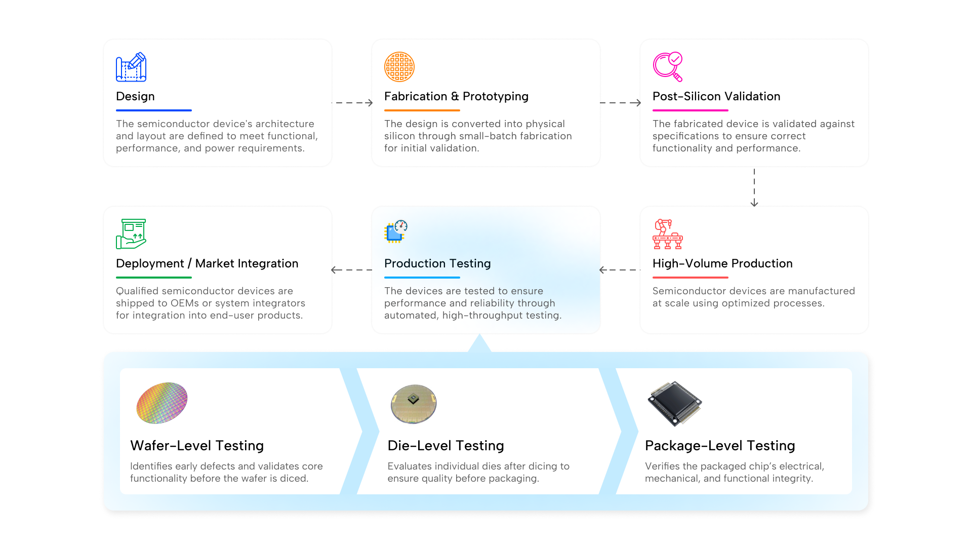
  • Manual orchestration across test stages: Engineers must independently coordinate testing across wafer, die, and package levels, often relying on custom scripts and manual setup replication. 
  • Inconsistent procedures and redundant scripting: The absence of standardization across teams and ATE platforms results in variability in test quality and repeated effort in developing similar test logic for different stages or tools. 
  • Disjointed data flows: Test data is isolated at each stage, making cross-stage correlation, early anomaly detection, and root cause analysis difficult. This hinders coordination and real-time visibility across the workflow. 

To bridge these disparities, semiconductor manufacturing requires more than just automation at the hardware level. It requires a comprehensive software infrastructure that ties everything together by standardizing test execution, centralizing control, enabling data-driven insights, and unifying operations across all stages of testing.  


How Automation and Software Infrastructure are Reshaping Semiconductor Manufacturing 

The integration of a comprehensive software infrastructure and automation brings transformative impacts to semiconductor manufacturing: 

  • Increased Throughput & Reduced Cycle Times 

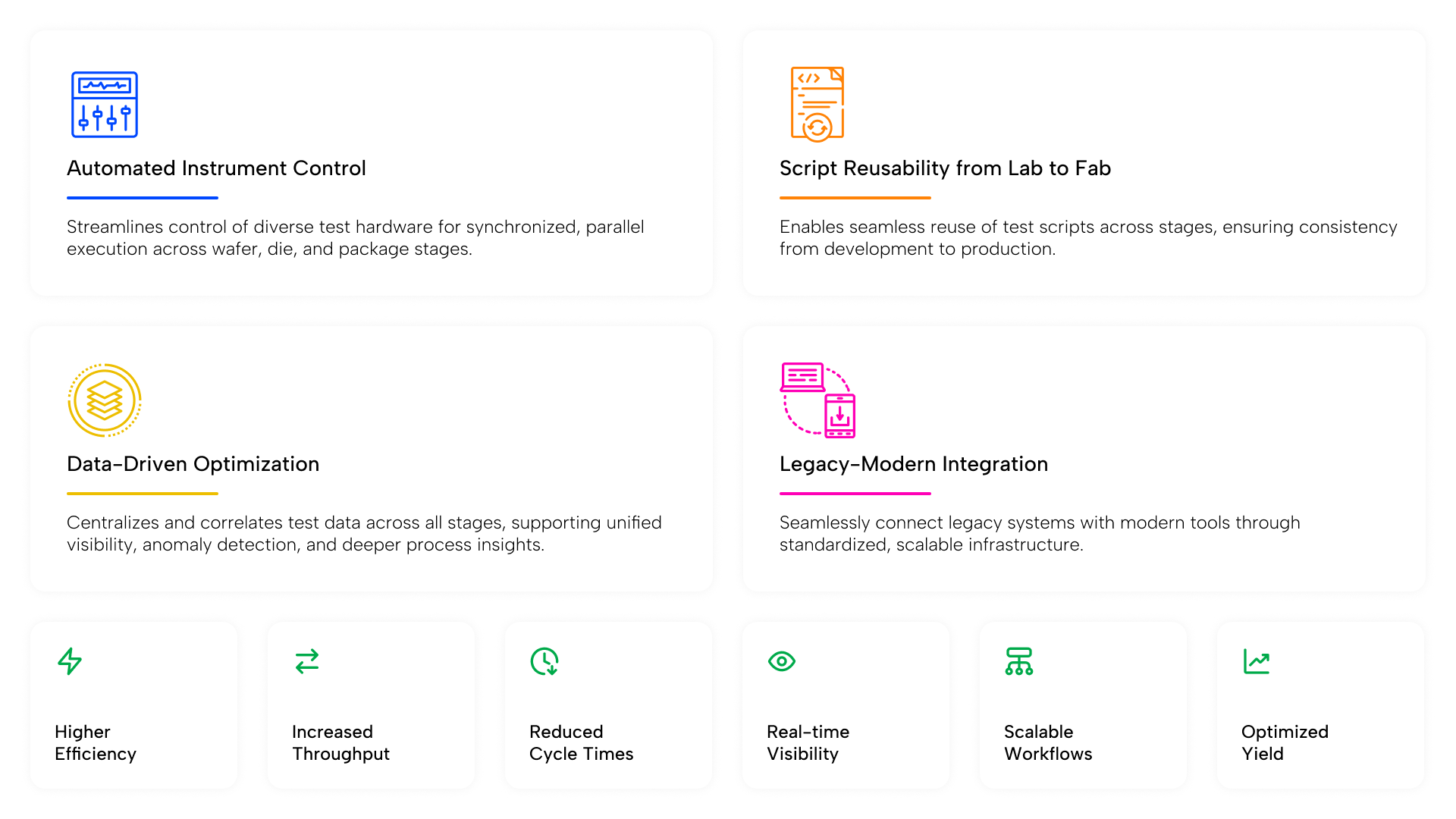
Automation and robust software infrastructure eliminate manual intervention by orchestrating test setups, automating instrument control, and aggregating real-time test data throughout production. Parallel execution of multiple test routines and intelligent scheduling optimize equipment utilization, enabling faster validation of thousands of chips per hour while maintaining precision. 

  • Enhanced Quality & Consistency 

Standardized test execution and centralized control ensure that every device is evaluated under uniform conditions, minimizing human error and setup variations. Automated test sequences run predefined conditions with real-time anomaly detection, reducing defect rates and enhancing long-term reliability so that every batch meets the highest performance standards. 

  • Expanded Test Coverage & Script Reusability 

With a unified automation framework, test scripts created in one stage can be reused in another. For example, test scripts developed during bench validation can be seamlessly reused in high-volume production. This eliminates redundant scripting across stages and platforms, ensuring methodological consistency and standardization from lab to fab and significantly reducing engineering effort. 

As part of a Lab-to-Fab initiative with Analog Devices Inc., we enabled enterprise-wide standardization in semiconductor validation and characterization. The infrastructure bridged bench validation and high-volume production, with reusable test scripts driving a 30% efficiency boost in the overall process. 

Learn more about our partnership and the impacts we created.  

  • Data-Driven Process Optimization 

Centralized data collection and correlation across stages unlock actionable insights, enabling engineers to detect yield fluctuations, process drifts, and equipment inefficiencies in real-time. AI-powered analytics further enhance this by identifying failure patterns and predicting potential defects, enabling proactive, yield-improving interventions. 

  • Bridging the Gap Between Legacy and Modern Systems 

Integrating legacy systems with modern processes remains a significant hurdle in semiconductor manufacturing. A well-designed automation infrastructure, built on standardized protocols like GEM and microservice-based architectures, ensures interoperability across generations of test hardware. This allows gradual upgrades while maintaining a unified, disruption-free production environment. 


Experience Test and Measurement Software Expertise with Automation for Your Manufacturing Workflows    

At Soliton, our mission is to empower semiconductor manufacturers with test automation solutions that seamlessly integrate advanced software, data analytics, and artificial intelligence with manufacturing hardware. Our expertise not only meets the current demands of semiconductor testing but also future-proofs operations as production scales and technology evolve. With our solutions and expertise, we optimize testing processes at every production stage, ensuring consistent quality, improved yields, and faster time-to-market.     

Partner with us and experience how our comprehensive expertise in test automation, data, and AI can drive unparalleled efficiency, quality, and scalability in your manufacturing operations.